SUMMARY
Keywords: Quantum Information, Spin Coherence, Condensed Matter, Solid State Qubits
This technology enables diamond to be integrated with other functional materials enabling the fabrication of diamond-based heterostructures, which are ideal hybrid systems for quantum networking and sensing.
The Unmet Need: Scalable production of diamond heterostructures for quantum applications
Diamond is a leading material platform in quantum information science with several landmark demonstrations in quantum sensing and quantum communication.
However, these demonstrations rely on devices carved directly into bulk, monolithic diamond at high cost, low throughput, and low yield, limiting scalability and device functionality.
For instance, millimeter scale electronic-grade diamond has limited availability and costs thousands of dollars. Additionally, device functionality is highly limited by the diamond material, which lacks any significant nonlinear optical response and is challenging to fabricate at the nanoscale without degradation of the optical and spin qubit properties.
To usher in the next phase of quantum technologies, diamond must be efficiently and effectively integrated with other functional materials.
The Proposed Solution: Bonding thin film diamond to heterogeneous substrates
The inventors have developed a method to directly bond sub-micron thickness single crystal diamond membranes to heterogeneous substrates (such as fused silica, thermal oxide, lithium niobate etc.) via plasma-activation of bonding surfaces.
The bonded device has great adhesion and flatness across the diamond region and is robust against many nanofabrication processes and surface treatments. With tunable membrane thickness and low optical background, this technology offers many opportunities for integrating diamond with many quantum and conventional technologies.
FIGURE
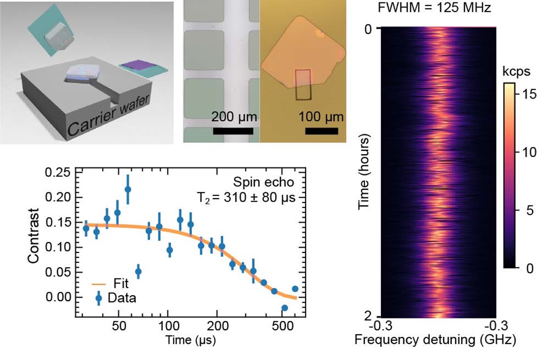
Tunable and transferable diamond membranes that host coherent quantum states
ADVANTAGES
Advantages
- Low flatness tolerance
- High double-sided parallelism
- Low height variation
- High crystal quality
- Low curvature
- Greater bonding strength and uniformity
- Compatibility with heterogeneous integration
- Strong mechanical performance
Applications
- Nanophotonic integration on a diamond-based hybrid system
- Bio-sensing with Nitrogen Vacancy Centers: microfluidic channel for molecule sensing
- Phonon-mediated interaction between color centers: Diamond-LiNbO3 hybrid system
- Novel superconducting qubit design with diamond as the dielectric material
- Other quantum sensing applications: bulk magnetic material, type II superconductors etc.
- Power electronic device: thin film diamond as the heat dissipation layer (better than SiC)
PUBLICATIONS
- Guo, X. et al. Microwave-Based Quantum Control and Coherence Protection of Tin-Vacancy Spin Qubits in a Strain-Tuned Diamond-Membrane Heterostructure. Phys Rev X 13, 041037 (2023). https://arxiv.org/pdf/2307.11916.pdf
March 6, 2024
Proof of concept
Patent Pending
Licensing,Co-development
Alexander High